Silicon On Insulator Wafer Fabrication

Silicon On Insulator Soi Wafers Silicon Valley Microelectronics

Silicon On Insulator Soi Wafers Size 4 Thickness 725 Um P Type Boron Doped Nanografi Nano Technology Teknoloji
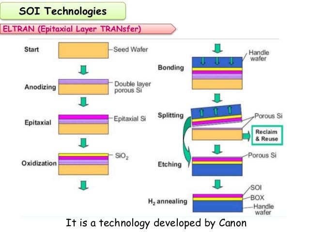
Silicon On Insulator Soi Technology

What Is A Silicon Wafer Silicon Valley Microelectronics

Silicon Fusion Bonding Process Showing The Deformation Of Silicon Wafers Download Scientific Diagram

Double Soi Fabrication Process Showing Wafer Bonding And Substrate Download Scientific Diagram

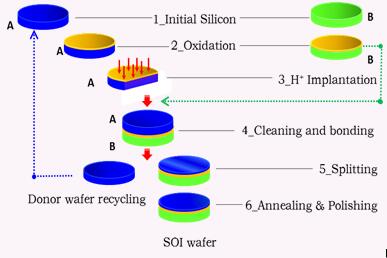
We propose a process for the fabrication of a silicon on insulator soi wafer with a silicon carbide sic insulator layer by combining plasma enhanced chemical vapor deposition and surface activated bonding without thermal stress to obtain sufficient thermal conductivity for self heating power and high frequency device applications.
Silicon on insulator wafer fabrication.

Pdf Silicon On Insulator Technology Review

What Is A Silicon Wafer What Is It Used For Waferpro
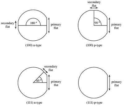
What Is The Orientation Of Silicon Wafer 100 111 110

What Are Prime Test Dummy And Reclaimed Grade Silicon Wafers

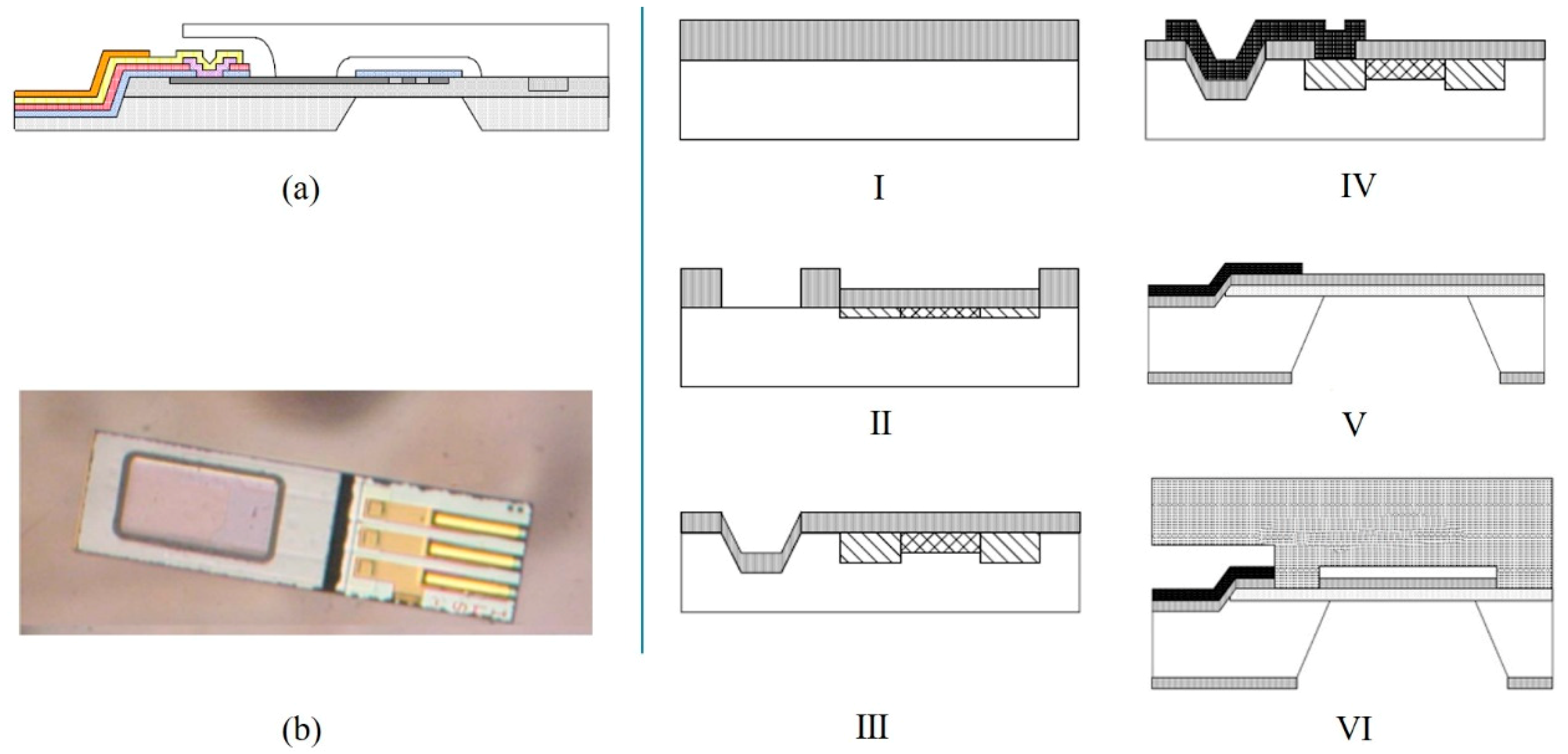
Fabrication Process Of Device In Silicon Layer Of Soi Wafer A Device Download Scientific Diagram

Abbreviated Double Soi Fabrication Process Showing Second Wafer Bonding Download Scientific Diagram

Bonded And Etchback Soi Waferpro

Fabrication Process Flow A 30 Mm Soi Wafer B Deposition Of A 0 75 Download Scientific Diagram

Silicon Wafer Supplier Waferpro Waferpro

Silicon Wafer An Overview Sciencedirect Topics

Pressure Sensor Chip Fabricated In Soi Technology 1 A Pure Silicon Download Scientific Diagram

Fabrication Flow Diagram For Sinwfet A Soi Wafer B Oxidation C Download Scientific Diagram

Zinc Telluride Single Crystal Substrate In 2020 Substrate Zinc Crystals

Silicon Wafer Reclaim Services Wafer Semiconductor West Palm Beach
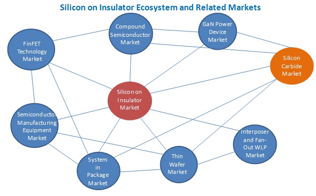
Silicon On Insulator Soi Market By Wafer Size Wafer Type Technology Product Covid 19 Impact Analysis Marketsandmarkets

Fabrication Sequence A Soi Wafer Preparation B Piezoresistor Download Scientific Diagram

The Prior Art Of Micro Pressure Sensors Fabricated On Soi Wafers Download Scientific Diagram
Https Encrypted Tbn0 Gstatic Com Images Q Tbn 3aand9gcsjqiivyvqyyw5jykmda Sy Dxfukqsocua4fqzha1xfqbobdr6 Usqp Cau

Fabrication Process Of The Proposed Flexible Neural Probe A Starting Download Scientific Diagram

Soi Fabrication Process A Soi Wafer With 50 µm Device Layer 3 µm Download Scientific Diagram

Fabrication Process Flow A 4 100 P Doped Boron Soi Wafer With Download Scientific Diagram

Fabrication Process Of A Silicon Resonator On The Ltcc Substrate With Download Scientific Diagram

Process Flow For Cmos Compatible Fabrication Of Monocrystalline Silicon Download Scientific Diagram

Plasma Activated Direct Bonding Of Patterned Silicon On Insulator Wafers To Diamond Coated Wafers Under Vacuum Sciencedirect

Sic Power Device Market To Grow At 40 Cagr From 2020 To More Than 1bn In 2022 After Tipping Point In 2019 Power Marketing Semiconductors

About Silicon Wafers Waferpro

Semiconductor Market Will Recover In 2017 Semiconductor Marketing Semiconductors

Power Gan Device Ip Dynamics Heralds Future Ramp Up Of Market Power Marketing Semiconductors

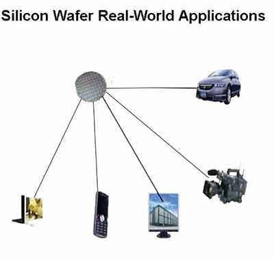
Ilicon Wafers Application

Thick Film Silicon On Insulator Wafers Preparation And Properties Sciencedirect
Silicon Wafer Semiconductor Research Applications
Https Mems Eng Uci Edu Files 2018 11 J57double Sided Process For Mems Soi Sensors With Deep Vertical Thru Wafer Interconnects Pdf

Trenches Differing In Widths And Depths On The Normal Silicon Wafer A Download Scientific Diagram
Micromachines Free Full Text Recent Progress Of Miniature Mems Pressure Sensors Html
Ppt The Many Processes Of Silicon Wafer Processing Powerpoint Presentation Id 7483080
Thick Film Soi Wafers Preparation And Properties Sciencedirect

Silicon Wafer Bonding Technology For Vlsi And Mems Applications Emis Processing Series 1 Subramanian S Iyer Subramanian S Iyer Andre J Auberton Herve 9780852960394 Amazon Com Books

Pokemon Home A New Cloud Storage Service In The Vein Of Pokemon Bank For 3ds Is Set To Launch On In 2020 Pokemon Nintendo Nintendo Switch News

Semiconductor Wafers Silicon Wafers Manufacturer From Bengaluru

Fabrication Of The Nr Isfet Chips A Soi Wafer Tsoi 200 Nm Tbox Download Scientific Diagram

Bare Silicon Wafers Advantiv Technologies Inc
Https Iopscience Iop Org Article 10 7567 1347 4065 Aaea6d Pdf
Https Encrypted Tbn0 Gstatic Com Images Q Tbn 3aand9gctgxojlnbp8st7cg2doynyb Tlrgrrr76wqtob2lemouskyuvta Usqp Cau
Source : pinterest.com
