Silicon On Insulator Wafers

Silicon On Insulator Soi Wafers Size 4 Thickness 725 Um P Type Boron Doped Nanografi Nano Technology Teknoloji

Diced Soitec Silicon On Insulator Wafers Wafer Semiconductor Materials Insulation

What Are Soi Wafers Or Silicon On Insulator Wafers How To Introduce Yourself Innovation Technology Insulation

Growing Product Demand For Consumer Electronics Devices Driving Silicon On Insulator Market In 2020 Insulation Marketing Semiconductor

Silicon On Insulator Market Forecast 2026 2019 Global Rf Soi That Support Data Transfer Rates Of 1 Gbps And H Technology Trends Insulation Media Communication

Silicon On Insulator Soi Market Insulation Marketing Semiconductor

Svm is a silicon wafer supplier that sells high grade factory sealed silicon wafers these are available from our stock in every diameter with an emphasis on 100mm 200mm and 300mm test device quality wafers.
Silicon on insulator wafers.

4 Inch Silicon Wafer Silicone Wafer Stuff To Buy

Pin On Semiconductors

Silicon On Insulator Market In 2020 Drupal Crypto Money Development

Silicon Wafer Cassette Wafer Semiconductor Materials Semiconductor

Silicon Wafer Reclaim Services Wafer Semiconductor West Palm Beach
Silicon On Insulator Soi Wafers Size 6 Device Thickness 625 Nm P Type Radyo Verimlilik

Zinc Telluride Single Crystal Substrate In 2020 Substrate Zinc Crystals

Matchless Silicon Wafer Manufacturers Wafer Semiconductor Manufacturing

Sic Power Device Market To Grow At 40 Cagr From 2020 To More Than 1bn In 2022 After Tipping Point In 2019 Power Marketing Semiconductors

Next Big Future 4ds Memristor Achieves Technical Milestone Of Memory Cells Denser Than 3d Flash With Commerciallization In The 2019 Tim

Thermal Oxide On Silicon Wafer Thermal Wafer Semiconductors

Pin De Nina Mehrkens Em Industry News Engine Iphone Componentes Tecnologia

Power Gan Device Ip Dynamics Heralds Future Ramp Up Of Market Power Marketing Semiconductors

Silicon On Insulator Soi Market Insulation Marketing Semiconductor

Silicon On Insulator Soi Market Insulation Marketing Semiconductor

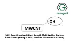
Graphitized Multi Walled Carbon Nano Tubes Purity 99 99 Outside Diameter 28 48nm Nanografi Nano Technology

Pin On General

Ibm News Room 2017 06 05 Ibm Research Alliance Builds New Transistor For 5nm Technology United States Ibm Technology Research

Mdc Is Proud To Sponsor The 2018 Confab Executive Conference The Confab Brings Together Influential Decision Maker Networking Event Gas Delivery Semiconductor

Ptu0415 Platinum Crucible Mold Replacements For Vulcan Crucible Electric Furnace Platinum

Pin On Mdc Gas Delivery Products Division

Best Deals And Free Shipping Ebay Amd Technology

Drive Your Semiconductor Process Forward With Vacuum Ceramic Seal And Gas Delivery Product Solutions From Mdc Gas Delivery Semiconductor Ceramic Materials

Graphene Tantalum Create High Density Memory Boost Memory Technology High Density Storage

Leveraging Quantum Tunneling Effects In Graphene Joshbyard Contact Lenses Infrared Semiconductors

Graphene And Health Impacts Science Materials Science Nanotechnology

Cubic Close Packed Structure Google Search Chemistry Simple

Pvd Ito Physical Vapor Deposition Physics

Pin Taulussa Amazon

The Mdc Vacuum Limited Mdc Europe Division Of Mdc Vacuum Products Llc Is Your One Stop Shop For Vacuum Science Solutions Vacuums Shop Vacuum Finite Element

Semiconductor Market Will Recover In 2017 Semiconductor Marketing Semiconductors
Mdc Can Take Your Design From Prototype To Serial Production While Maintaining Superior Workmanship Along The Way So Gas Delivery Vacuums Alternative Energy

The Computer Industry S Future Depends On A Behind Schedule Technology That S Proving Tough To Engineering Technology Technology Review Electrical Engineering

Integrated Circuit Microcontroller Flash Atmega328 Atmega Microcontrollers Aliexpress Circuit

Nanosolar Technology Overview

Buy Graphene Online And Save Wafer Substrate Stuff To Buy

Leveraging Quantum Tunneling Effects In Graphene Joshbyard Contact Lenses Infrared Semiconductors

Congratulations Mdc Raffle Prize 3 Winner In 2020 Semiconductor How To Apply Raffle

Understanding Quantum Photovoltaics Solar Panels Solar Energy Best Solar Panels

Gecko Like Adhesives Now Work On Real World Surfaces Surface Material Science Physics Research

We Had A Great Time At Semicon West Last Week Thank You To All Those We Took The Time To Stop By Our Booth And Semiconductor Technology Semiconductor Vacuums

Integrated Circuit Microcontroller Flash Atmega328 Atmega Microcontrollers Aliexpress Circuit

Nanosolar Technology Overview

Pin Em 3d
Source : pinterest.com
